Suzhou Kaifa New Material Technology Co., Ltd.
Email:heqing@szkfxc.com
Email:sales@szbknm.com
Email:bkxc.bonnie@gmail.com
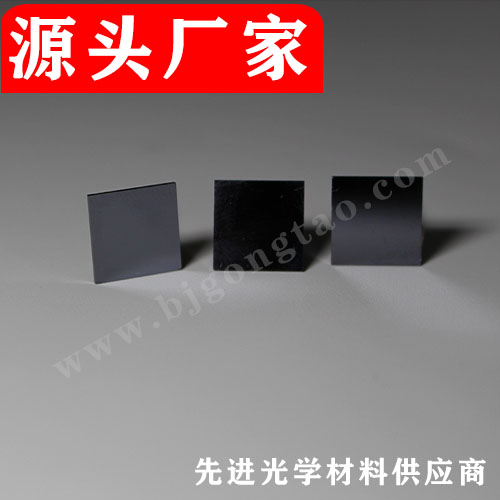
SEM single crystal silicon wafer double-sided polishing experiment scientific research high purity single crystal silicon wafer size can be customized
Email:beikenano@gmail.com
Email:beikenano@gmail.com
Monocrystalline silicon wafer (double-sided polishing)
Features: High purity silicon si single crystal substrate, N / P type optional, resistivity 0.0001-100 ohm, optional
Growth mode: straight pull
Crystal orientation: [111] / [100] / [110]
Flatness: <1 micron (measure the overall warpage)
Surface roughness: about 5 angstroms (measure the surface micro-topography)
Uses: 1. PVD / CVD coating as substrate
2. Used as XRD (X-ray diffraction analysis), SEM (scanning electron microscope), FTIR infrared, fluorescence spectrum analysis test substrate, AFM (atomic force microscope)
3. Sample carrier for synchrotron radiation experiment
4. The substrate for molecular beam epitaxial growth
5. Semiconductor lithography process, etc.
Remarks: Other sizes can be customized and invoiced.
Warm tips: Kaifa products are only used for scientific research, not for human body,different batches of products have different specifications and performance.The website pictures are from the Internet. The pictures are for reference only. Please take the real object as the standard. In case of infringement, please contact us to delete them immediately.
Quality AssuranceHigh standards of the industry-leading
|
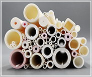
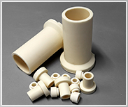
Ceramic tube Thermocouple protection tube |
|
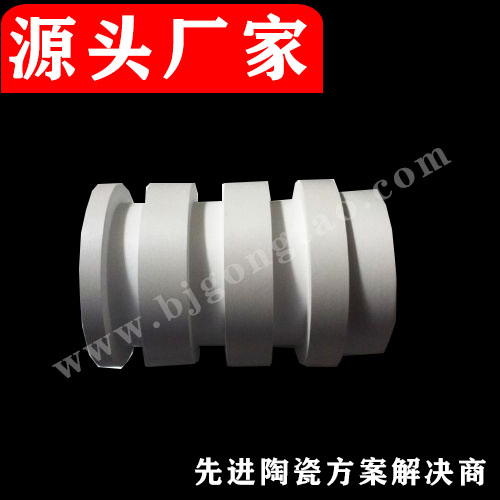
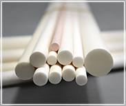
Ceramic rod Ceramic shaft sleeve insulated |
|
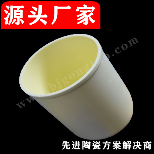
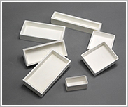
Ceramic crucible High quality and high temperature resistant |
|
T-shaped concave convex tube High temperature insulator porcelain mouth porcelain |
|
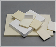
Ceramic plate Alumina plate, ceramic plate, bearing plate, |
|
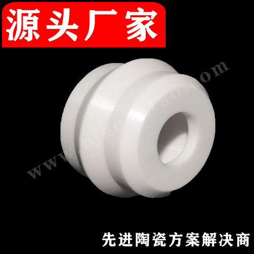
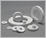
Ceramic gasket High temperature resistant ceramic ring, |
|
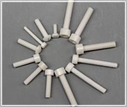
Screw nut Insulating screws, corrosion-resistant bolts, |
|
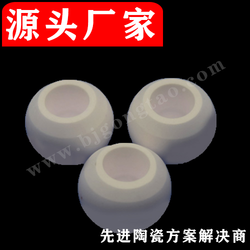
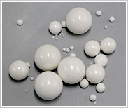
Ceramic ball Alumina and zirconia ultrafine grinding media. |

