
-
 Boron nitride ...
 -
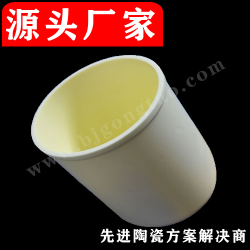
 Zirconia ceram...
 -
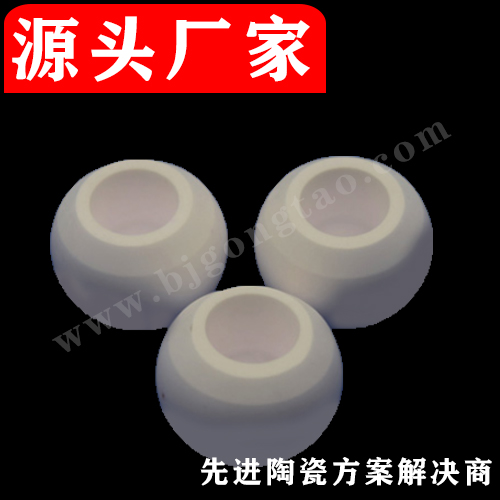 Ceramic ball
 -
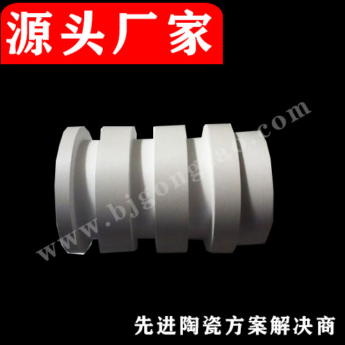
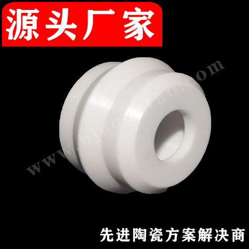
 99 alumina cer...

Suzhou Kaifa New Material Technology Co., Ltd.
Email:heqing@szkfxc.com
Email:sales@szbknm.com
Email:bkxc.bonnie@gmail.com
alumina ceramic problem
氧化铬陶瓷问题In recent years, with the rapid development of electronic technology, large-scale integrated circuits have been widely used, the functions of integrated devices have become increasingly complex, and the output power has continued to increase. Electronic equipment, especially related electronic products in the downstream industry chain of the Internet of Things, mobile phones, computers, smart homes, watches, sports bracelets, etc., due to the needs of miniaturization and mobility, require reduction of the packaging volume of devices, electronic equipment The structural design of the device is developing towards the direction of ultra-small assembly, and the packaging density of the device has also increased. At the same time, the power required to dissipate per unit area continues to increase, and the heat dissipated by electronic components increases correspondingly, and the heat flux density is also doubled. Increase. How to effectively reduce the temperature rise of electronic components, especially the temperature rise of electronic components in a sealed small volume, puts forward higher requirements for the packaging of electronic components.
Ceramic packaging substrates are packaging materials and are a key carrier in the packaging and testing process of the integrated circuit industry chain. They not only provide support, heat dissipation and protection for the chip, but also provide an electronic connection between the chip and the PCB. Packaging substrates account for about 46% of packaging materials and are key supporting materials in the integrated circuit industry chain. The application of advanced ceramics in electronic packaging has largely solved the problem of chip thermal management.
Advanced ceramic materials, also known as precision ceramic materials, refer to products with excellent performance that are manufactured using refined, high-purity, ultra-fine inorganic compounds as raw materials and advanced preparation technology. Alumina (Al2O3) ceramics have the advantages of abundant raw materials, low price, high insulation, heat shock resistance, chemical corrosion resistance and high mechanical strength. It is a ceramic substrate material with good comprehensive performance, accounting for the total ceramic substrate materials. More than 80% of the amount. The Rockwell hardness of alumina (Al2O3) ceramics is HRA80-90 determined by the Shanghai Institute of Ceramics, Chinese Academy of Sciences. The hardness is second only to diamond and far exceeds the wear resistance of wear-resistant steel and stainless steel. Measured by the Institute of Powder Metallurgy of Central South University, the wear resistance of alumina (Al2O3) ceramics is equivalent to 266 times that of manganese steel and 171.5 times that of high-chromium cast iron. The density of alumina (Al2O3) ceramics is 3.5g/cm3, which is only half of that of steel, which can greatly reduce equipment load.
Ceramic substrates can just meet the performance requirements of mid-to-high-end chips, and have been well applied in mid-to-high-end products in the fields of home appliance lighting, information communication, sensors and other fields. It is an ideal packaging material for a new generation of large-scale integrated circuits and power electronic modules. . The use of ceramic substrates has provided impetus for the electronics and semiconductor industries. Stone alumina ceramic substrate adopts DPC thin film technology, and the copper and ceramic substrate are firmly combined by magnetron sputtering method. The ceramic circuit board has good metal crystallization performance, good flatness, and the circuit is not easy to fall off, and it is reliable and stable. The performance, thereby effectively improving the bonding strength of the chip and the substrate.
The alumina ceramic substrate can be assembled with high density (line/spacing (L/S) resolution can reach 20μm) and supports customized drawings. It is a good helper for equipment integration and miniaturization in the Internet of Things environment.
