
-
 Boron nitride ...
 -
 Zirconia ceram...
 -
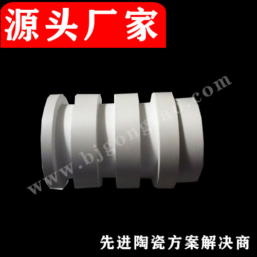
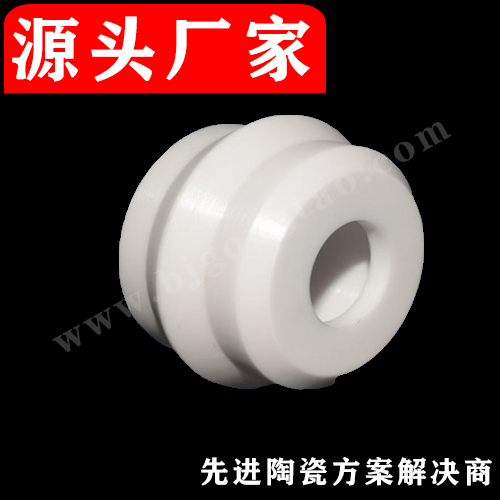
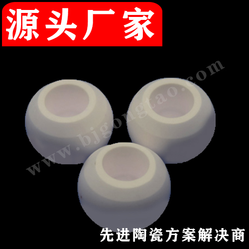 Ceramic ball
 -
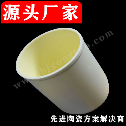 99 alumina cer...

Suzhou Kaifa New Material Technology Co., Ltd.
Email:heqing@szkfxc.com
Email:sales@szbknm.com
Email:bkxc.bonnie@gmail.com
Five major surface metallization processes of alumina ceramics
Alumina is a well-known and commonly used precision ceramic material. For decades, it has been used in electrical components because of its high electrical insulation. It is widely used in our life due to its high strength, high corrosion resistance and high wear resistance. Because alumina is a material with relatively balanced mechanical properties, alumina is widely used, including wear-resistant products used in high-temperature industrial furnaces and various electronic components. Alumina ceramic substrates are widely known as a precision ceramic material due to their stable chemical and physical properties.
Alumina ceramics are divided into two types: high-purity type and ordinary type
High-purity alumina ceramics refers to ceramic materials with Al2O3 content of more than 99.9%. Because of its sintering temperature as high as 1650-1990 °C and transmission wavelength of 1-6 μm, it is generally made into molten glass to replace platinum crucibles; It can be used as a sodium lamp tube with light properties and alkali metal corrosion resistance; it can be used as an integrated circuit substrate and a high-frequency insulating material in the electronics industry.
Ordinary alumina ceramics are divided into 99 porcelain, 95 porcelain, 90 porcelain, 85 porcelain and other varieties according to the content of Al2O3. Sometimes those with Al2O3 content of 80% or 75% are also classified as ordinary alumina ceramics series. Among them, 99 alumina ceramic materials are used to make high-temperature crucibles, refractory furnace tubes and special wear-resistant materials, such as ceramic bearings, ceramic seals and water valve plates; 95 alumina ceramics are mainly used for corrosion-resistant and wear-resistant parts; 85 ceramics Because part of talc is often mixed into it, the electrical properties and mechanical strength are improved, and it can be sealed with metals such as molybdenum, niobium, and tantalum, and some are used as electric vacuum devices.
Alumina ceramic surface metallization process
Because of its good electrical properties, alumina ceramics are the most widely used in electrical and electronic applications, and as an electronic and electrical substrate material, the surface metallization must be involved. Because ceramics are insulating materials, only the surface metallization is required. to conduct electricity.
Ceramic metallization is to firmly adhere a layer of metal film on the surface of the ceramic, so that it can realize the welding between the ceramic and the metal. The more advanced application is to form a circuit on the surface of the ceramic, which can not only be welded, but also can be used as a wire to transmit current. At present, the traditional metallization methods include thick film method, DBC method, DPC method, LTCC and HTCC. The advantages and disadvantages of these processes are explained below one by one:
01 Thick film method
By screen printing, various circuits, resistors and capacitors are printed on the ceramic base. It is undeniable that this process is widely used and can carry large currents. Most of the applications of ceramics are realized by the thick film method, but Can it really cure all diseases? We all know that the accuracy of screen printing is very unsatisfactory, and the combination of silver paste and ceramics cannot reach a satisfactory level. At the same time, silver paste needs to be sintered at a certain temperature to solidify. These shortcomings are believed to have Many people in the industry have also been deeply troubled. Moreover, the thick film method has thicker lines, which is a big obstacle to the miniaturization of electronic products, so everyone has to come up with other methods.
02 D B C method
This process is often used in high-power modules. The copper layer is thicker and can carry larger currents. It has good thermal conductivity, high strength, and strong insulation. The thermal expansion coefficient matches that of semiconductor materials such as Si. However, the reactivity of ceramic substrates and metal materials is low, and the wettability is poor. It is difficult to implement metallization, and it is difficult to solve the problem of micro-pores between Al2O3 and copper plates. In addition, the high sintering temperature and high cost can only be applied to areas with special needs.
03 OPC method
It is widely used in the field of LED, and the technology is mainly in the hands of Taiwanese manufacturers. Tongxin Electronics accounts for more than half of its annual shipments. In addition, there is Aisibo. The major advantages of this process are high circuit precision, smooth surface, and relatively It is suitable for flip-chip/eutectic packaging. International LED manufacturers such as Cree and Osram are using Tongxin‘s substrates. Its cost is lower than the DBC method, and the DPC technology of Slitton has been officially mass-produced in China.
04 L T C C
Because LTCC uses thick film printing technology to complete the circuit production, the surface of the circuit is relatively rough and the alignment is not accurate. Moreover, the multi-layer ceramic lamination and sintering process also has the problem of shrinkage ratio, which limits its process resolution and greatly challenges the promotion and application of LTCC ceramic substrates.
05 HTCC
Due to the high sintering temperature, this process has very few users and is basically replaced by LTCC.
